Integrated Circuit
WHAT IS INTEGRATED CIRCUITS ?
• A complex set of electronic components and their interconnections that are imprinted onto a tiny slice of semiconducting material.
• Integrated Circuits are usually called ICs or chips.
•Integrated circuits were made possible by experimental discoveries which showed that semiconductor devices could perform the functions of vacuum tubes and by mid20th-century technology advancements in semiconductor device fabrication.

• The integrated circuit's mass production capability, reliability, and building-block approach to circuit design ensured the rapid adoption of standardized ICs in place of designs using discrete transistors.


History of ic
An IC also refered as chip or micro chip is a set of electronic circuits on one small chip of semiconductor material, normaly silicon.
This can be made much smaller than a discreet circuit made from independent electronic components. IC’s can be made very compact having up to several billion transistors and other electronic components in an area the size of a fingure-nail.
The width of each conducting line in a circuit can be made smaller and smaller as a technology advances; in 2008 it dropped below 100 nanometers and has now being reduced to tens of nanometers.


Monolithic IC’s
A Monolithic Microwave Integrated Circuit, or MMIC is a type of integrated circuit (IC) device that operates at microwave frequencies.
These devices typically perform functions such as microwave mixing, power amplification, low-noise amplification, and high-frequency switching.
Inputs and outputs on MMIC devices are frequently matched to a characteristic impedance of 50 ohms. This makes them easier to use, as cascading of MMICs does not then require an external matching network.

Thick & Thin Film IC’s
The general characteristic, properties, and appearance of thin and thick-film integrated circuits are similar, although they both differ in many respect from monolithic integrated circuits.
They are not formed within a semiconductor wafer but on the surface of an insulating substrate such as glass or an appropriate ceramic material.
The primary difference between the thin-and-thick-film techniques is the process employed for the forming the passive component and the metallic conduction pattern.
The thin-film circuit employs an evaporation or cathodes-puttering technique; the thick film employs silk-screen techniques.

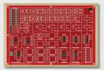

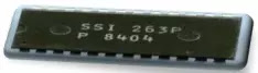
SSI
MSI
LSI
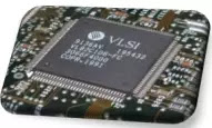
VLSI
VVLSI
WSI
NANO TECHNOLOGY
Scale of integration
Small Scale Integration (SSI)
Normally it has about 20 components.
The Minuteman missile and Apollo program needed lightweight digital computers for their initially-guided flight computers.
The Apollo guidance computer led and motivated the integrated-circuit technology, while the Minuteman missile forced it into mass-production.

Medium Scale Integration (MSI)
It can have about 100 components.
Medium Scale Integration came in to industry in late 1960s.
MSI is the next step in the development of integrated circuits after 'Small Scale Integration'.
Medium-Scale Integration allowed more complex systems to be produced using smaller circuit boards than in SSI (Small Scale Integration).
It have about 1000 components.
LSI is the process of integrating or embedding thousands of transistors on single silicon semiconductor microchip. LSI technology was conceived in mid-1970s when computer processor microchips were under development


Very Large Scale Integration (VLSI)
Very large scale integration.
It can have about 10,000 components.
VLSI began in the 1970s ,when complex semiconductor and communication t echnologies were being developed.

Very Very Large Scale Integration(VVLSI)
Very Very Large Scale Integration
Also known as Ultra large scale integration.
It can have about 10million components.
The ability to pack more electronic components onto a chip increases the computational power and speed of the computer or other machine in which the chip resides.


Wafer Scale Integration(WSI)
The evolution in semiconductor technology that builds a gigantic circuit on an entire wafer.
Just as the integrated circuit eliminated cutting apart thousands of transistors from the wafer only to wire them back again on circuit boards, wafer scale integration eliminates cutting apart the chips.


Nanotechnology
Nanotechnology, in the context of computer science, is a type of engineering geared toward building electronic components and devices measured in nanometers, which are extremely tiny in size and structure.
Nanotechnology facilitates the building of functional matter and systems at the scalar level of an atom or molecule.
Nanotechnology is also known as Nanotech. Explains Nanotechnology
Nanotechnology works through different approaches to build nano materials or products, including bottom-up, top-down and Functional system development.
In a bottom-up approach, a product is designed as it evolves from its tiniest form factor to larger product.
In a top-down approach, a large product may be reverse engineered to develop products scaled according to nanometer.
A functional approach deals with a complete system and may incorporate bottom-up and top-down approaches.
Explains Nanotechnology
Nanotechnology works through different approaches to build nano materials or products, including bottom-up, top-down and Functional system development.
In a bottom-up approach, a product is designed as it evolves from its tiniest form factor to larger product.
In a top-down approach, a large product may be reverse engineered to develop products scaled according to nanometer.
A functional approach deals with a complete system and may incorporate bottom-up and top-down approaches.


Advantages of IC’s
1. Very small size
2. Low cost
3. Reduce power consuption
4. Highly reliable
5. Higher operating speed
6. Reduced external wiring connections
7. Easy to use
Disadvantages of IC’s
1. Component dependent
2. Limited capitance
3. Impossible to fabricates transformers
4. Limited power supplies
5. Not flexiable

Single Inline Packaging (SIP)
A single in-line (pin) package (SIP or SIPP) has one row of connecting pins. It is not as popular as the DIP, but has been used for packaging RAM chips and multiple resistors with a common pin. SIPs group RAM chips together on a small board either by the DIP process or surface mounting SMD process.
Dual Inline Packaging (DIP)
A dual in-line package is an electronic component package with a rectangular housing and two parallel rows of electrical connecting pins. The package may be through-hole mounted to a printed circuit board or inserted in a socket.
Zigzag Inline Packaging
The zigzag in-line package or ZIP was a short-lived packaging technology for integrated circuits, particularly dynamic RAM chips.
A ZIP is an integrated circuit encapsulated in a slab of plastic with 20 or 40 pins, measuring (for the ZIP-20 package) about 3 mm x 30 mm x 10 mm.
The package's pins protrude in two rows from one of the long edges. The two rows are staggered by 1.27 mm (0.05"), giving them a zigzag appearance, and allowing them to be spaced more closely than a rectangular grid would allow
Zigzag Inline Packaging